Today, a new technology exists at the intersection of AM and micro manufacturing, opening up the possibility for manufactures to take advantage of the inherent advantages of AM while achieving micron level accuracy over a build envelope of 5 x 5 x 10cm.
A Disruptive AM Technology for Micro Manufacturing
Jon Donner | Nanofabrica
There are two current global trends in manufacturing. The first is the trend towards miniaturization demanding parts and components with highly precise micron and sub-micron level resolution, and the other is the move towards digital manufacturing today referred to as Industry 4.0. Additive Manufacturing (AM) is a key enabling technology catering for the move towards shorter product life cycles, and allowing mass customization. The low set up costs associated with AM when compared to traditional manufacturing processes explains why it is now an established manufacturing technology adopted by a growing number of blue-chip companies across the world. Today, a new technology exists at the intersection of AM and micro manufacturing, opening up the possibility for manufactures to take advantage of the inherent advantages of AM while achieving micron level accuracy over a build envelope of 5 x 5 x 10cm.
The discipline of Additive Manufacturing (AM) or 3D Printing (3DP) is regularly cited as being disruptive to traditional manufacturing processes. Indeed there are existing AM production applications today across varied vertical sectors that support this position, optimised components and parts that would be either impossible or uneconomic to produce using traditional methodologies being made using AM technologies. In this way AM is truly disruptive and promotes innovation across numerous industry sectors.
A micro gear made from ABS used in an inkjet wideformat industrial 2D printer. Part size 1.3 x 1.3 x 0.4mm3, print time 35 minutes, and print layer 2 microns.
For some OEMs throughout the automotive, aerospace, medical (and a variety of other markets), AM has already become an established production and some instances mass manufacturing technology. However, for some barriers to entry for adoption of AM as a production technology still exist, key among these being the requirement for high initial capital investment and expensive on-going running costs; consumable costs (particularly for refined materials); inconsistent material properties which are a significant prohibitor for critical components; extensive pre-and post-processing requirements (and costs); and, often, a failure to understand when and how to apply AM to maximize its benefits.
The final reason is the focus of much attention today. AM has made the shift from a prototyping technology to a true production technology, but many lack the insight about what can really be produced on AM platforms, and the inherent characteristics of the process that add significant advantages when it come to cost, complexity, and timeliness of manufacture.
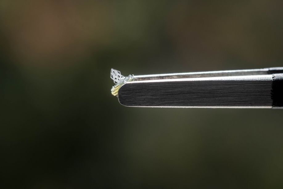
A diamond shaped lattice in ABS, a shape that is only possible to manufacture using additive manufacturing, and impossible using CNC machining or injection molding. The structure has ultra-high surface area and is therefore useful in heat dissipators. Part size 0.3 x 0.3 x 1mm3, print time 45 minutes, and print layer 3 microns.
It seems likely that the manufacturers of additive platforms are aware of this barrier to adoption, as many — mainly at the high-end of the system spectrum — have been refining and developing their respective processes by adding value propositions pre-, in- and post-process specifically for production applications. The corresponding vernacular that has emerged and is increasing in use across AM marketing campaigns and in-depth conversations about AM for production applications is “end-to-end manufacturing solutions.”
In addition, serious players in the AM sector are seeking out niches that are either under-served, or indeed in some instances completely un-served. One such is the area of micro manufacturing which until recently has had no viable AM technology that can reach the resolutions required,
When viewed from the perspective that across industry today there is an inexorable shift towards miniaturisation, with many applications demanding extremely exacting levels of micron and sub-micron precision on macro and micro parts, there is huge potential for an AM platform that can service this trend . A whole raft of traditional production platforms have developed to cater for this demand, but until recently, the ability for AM to produce such precision at all —let alone at volume production levels — has been impossible.
An AM platform Tailored for Micro / Nano Manufacturing
Nanofabrica, founded in 2016, has recently developed a micron-level resolution AM platform for this sector. The company has produced a technological solution that provides an end-to-end solution bespoke to manufacturers requiring micron and sub-micron levels of resolution and surface finish.
To date, key AM platform developers struggle to get resolution under 50 microns, and the few companies that have strived to provide a micro manufacturing AM solution are either extremely expensive in terms of machine costs and cost per part, or extremely slow, or can only print parts that are very restricted in size.
Successful AM platform developers in today’s crowded market need to focus technological advances on areas that open up innovation and the manufacture of products and components hitherto impossible using AM. It is here that Nanofabrica has been particularly successful, having identified a series of killer applications where there is burgeoning market demand, where the only route to market at the moment is through disproportionately expensive or restrictive traditional manufacturing technologies, and where the use of AM can open up significant advances on terms of design and functionality.
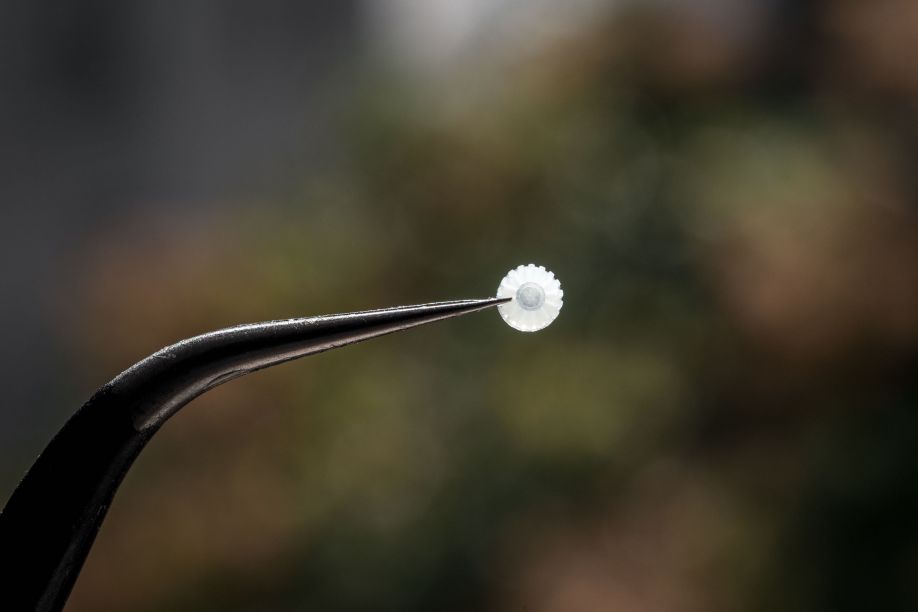
A micro honeycomb structure in PP, with wall thicknesses of ~20 microns over a height of a few mm. The part is made for a company that specializes in micro batteries. The ultra-high surface area is used to increase battery storage with minimal footprint. Part size 1.6 x 1.8 x 2.3 mm3, print time 80 minutes, and print layer 2 microns.
These killer applications exist in the area of optics, semi-conductors, micro electronics, MEMS, micro fluidics, and life sciences. Products such as casing for microelectronics, micro springs, micro actuators and micro sensors, and numerous medical applications such as micro valves, micro syringes, and micro implantable or surgical devices.
Microfluidics is a good example of how a true micro AM technology can outcompete traditional manufacturing processes. Microfluidic channels are used to move incredibly small volumes of liquid, and many of them incorporate functioning components such as filters and pumps. Traditional micro manufacturing processes such as micro molding hugely limit the freedom of design for such microfluidic channels, and it is almost impossible to manufacture functional substructures in them using such processes. The Nanofabrica AM technology overcomes these barriers without compromising precision or quality.
How the Process Works
The first breakthrough of Nanofabrica’s technology enables high precision at a cost required for industrial manufacturing. Nanofabrica’s AM process is based on a technology that is well known in the AM world, namely a Digital Light Processor (DLP) engine, but to achieve repeatable micron levels of resolution combines DLP with the use of adaptive optics. This tool in conjunction with an array of sensors, allows for a closed feedback loop. This is the core element that enables Nanofabrica’s product to reach very high accuracy while remaining cost-effective as a manufacturing solution. Where all other AM platform developers in this space achieve precision through great hardware, Nanofabrica tackles this issue with software where solutions are easier, more robust, and less expensive. Adaptive optics have been used in other areas of technology, but this is the first time that they have been applied to an AM technology.
Another unique aspect of Nanofabrica’s AM platform is the ability to achieve micron resolution over centimeter-sized parts. To enable this, a number of technologies have been combined.
Specifically, the company has taken its innovative use of adaptive optics and enhanced this imaging unit with technology and know-how used in the semiconductor industry (where the attainment of micron and sub-micron resolutions over many centimetres is routine.) By working at the intersection of semiconductors and AM, Nanofabrica is able to build large “macro” parts with intricate micro details. It can also do this at speed by introducing a multi resolution strategy, meaning that the parts where fine details are required are printed relatively slowly, but in the areas where the details aren’t so exacting, the part is printed at a speeds 10 to 100 times faster. This makes the entire printing speed anything from 5 to 100 times faster than other micro AM platforms.
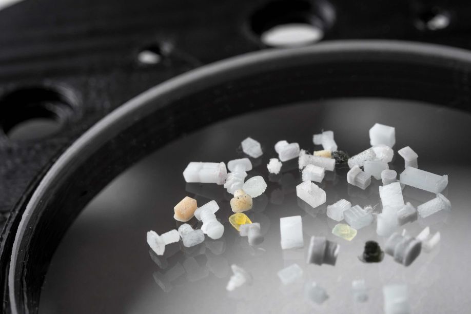
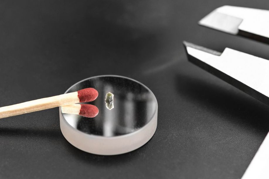
An array of parts made in various materials including 3 grades of ABS, 3 different grades of PP, as well as ceramic loaded parts.
In addition, for OEMs requiring small parts, thousands of parts can be printed in a single build on the Nanofabrica platform making it a true mass manufacturing technology for micro product or component manufacturers.
The multi resolution capability is possible through the use of hardware which enables a trade off between speed and resolution, and software algorithms which prepare the part and printing path by defining and sectioning it into low and high resolution areas, which are then fed into the printer path and machine parameters. Of course there are not only two resolutions but in fact a spectrum of resolutions that allow speed to be optimized while maintaining satisfactory results throughout the part.
The final algorithm family focuses on file preparation, optimizing parameters such as print angle build plate, supports etc…, which once again ensure a precise, optimized, and reliable print process.
Another major breakthrough at Nanofabrica is in the area of materials. Inherent in the company is a team with strong material development expertise, some leading executives in the company coming from material R&D backgrounds in the biggest and most successful companies in the AM arena. Through rigorous R&D, and using this expertise, Nanofabrica has managed to develop its own proprietary materials (based on the most commnly used industry polymers) which enable ultra high resolution in parts built.
What Does this Mean for Manufacturers
The Nanofabrica AM technology is a true blue ocean technology, meaning that in essence it is bringing AM into new markets and enabling new applications. For the first time, manufacturers that require micron and sub-micron level accuracy and resolution have an additive manufacturing technology available, and so for the first time, these manufacturers have the ability to benefit from the inherent advantages of AM.
Perhaps of key interest is the fact that AM is relatively agnostic to part complexity, and it is possible to design and manufacture unique geometries. As such, the Nanofabrica technology becomes an enabling technology, and a true stimulator of innovation, making the manufacture of parts and features previously impossible, possible.
AM also requires no set up costs. The tooling required for traditional manufacturing processes not only has a negative impact on time to market, but also makes such processes uneconomic for small or medium sized production runs. For AM technologies, small and medium sized runs are cost-effective, and indeed it is fair to say that today, represent the sweet spot for the technology.
Add into the mix that AM allows for mass customisation, personalization, and the ability to use the same manufacturing platform for prototyping, small batches, and mass manufacturing, and you begin to see the myriad of possibilities that now exist for micro manufacturers.
Technology Partner & Customized Solutions
Nanofabrica is aware — as the first mover in the micro AM space for production — that it establishes a partnership relationship with its customers that extends from product inception through to mass manufacturing. The technology is today the only micron-resolution platform aimed at true manufacturing applications not just R&D projects, the real game changer being the combination of commercially-oriented build volumes, optimised materials, significant lines of investment, and a platform that is competitively priced.
Beyond this however, Nanofabrica advocates close collaboration with customers to optimise outcomes. First and most importantly, the company offers expert design advice to ensure that designs are optimized for the technology.
As designer engineers and manufacturers assess the possibilities that exist for the use of AM to replace or, more likely, sit alongside traditional manufacturing processes, there needs to be a quantum shift in the way that they approach the entire design to manufacturing process.
Necessarily this begins with re-evaluating product design, and the subject of design for additive manufacturing (DfAM) has become a fertile area for discussion and debate today. Indeed, DfAM has become a bit of a “buzzword” in the AM space.
While AM users are beginning to take advantage of DfAM for macro AM platforms, there is little to no understanding of the DfAM issues when using AM for micro applications. It is because of this that Nanofabrica promotes a collaborative relationship with its customers to locate the opportunities and avoid the bear traps that exist when adopting — or considering adopting — AM for production purposes in the micro manufacturing arena.
Nanofabrica’s AM platform is relatively new to market, and today the company — through its collaborative ethos — is beginning to partner with key players in relevant sectors. By so doing, it is possible for Nanofabrica to customize the technology to precisely fit specific applications. For interested parties, the best way forward, and the way to ensure optimized use of this ground-breaking AM technology is to challenge Nanofabrica with a specific part, work on a proof of concept, and then install the technology either as a commercial manufacturing option, or embedded in an R&D project.
Summary
The history of manufacturing is characterized by leaps in technological developments. In the recent Industry 4.0 revolution, AM is a key technology and is a huge reason why digital manufacturing is replacing traditional manufacturing in many sectors.
AM has been a disruptive technology for a number of years, but until now it has not been able to achieve the exacting precision and resolution that is required by manufacturers at the forefront of miniaturizaton and micro manufacturing. The new Nanofabrica micro AM technology is ground-breaking in its ability to mass manufacture to micron-level resolution, and as such it appeals to an array of manufacturers that up until now have not been able to cost-effectively or efficiently fulfil design intent using traditional manufacturing processes.
Existing at the interface of AM for production and the industry-wide drive towards miniaturization, Nanofabrica’s micro AM technology lifts the lid for designers and manufacturers in their quest to embrace the inherent advantage of AM, and at last to be able to exploit the ability that exists with AM to build complex parts in small, medium, and high volumes in a timely and cost-effective fashion.
About Jon Donner
Jon Donner combines technical and business skills, and is now focused on making Nanofabrica an innovative and cost-effective solutions provider for manufacturers. Nanofabrica is Jon's second startup, having earned his PhD in nano optics in the Romain Quidant Plasmonics group at ICFO Barcelona, Spain. Before his PhD, he earned a double degree at TAU (Tel-Aviv University) in physics and electrical engineering and worked in an electro optics lab.
The content & opinions in this article are the author’s and do not necessarily represent the views of ManufacturingTomorrow
Featured Product