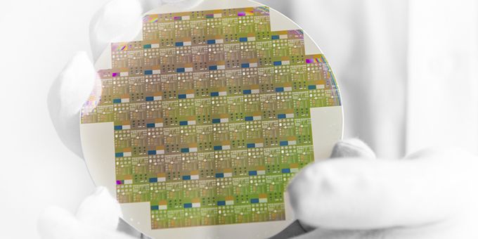
During manufacturing of integrated circuits (ICs), it is necessary to perform many deposition and etching steps to build the necessary internal structures. Among the most common are ashing, or stripping, to remove photoresist from etched wafers..
 Plasma Wafer Processing Tools
Contributed by | PVA TePla America
During manufacturing of integrated circuits (ICs), it is necessary to perform many deposition and etching steps to build the necessary internal structures. Among the most common are ashing, or stripping, to remove photoresist from etched wafers, as well as the “descum” process to remove any residue.
Although solvents can be used to remove photoresist in a “wet” process, alternatives that allow for dry processing are often sought out due to reducing chemical handling and acquisition costs. Among the alternatives for dry processing are plasma tools that apply ionized energy for wafer ashing and descum.
Although more advanced and automated, plasma etchers have been available since the earliest days of the semiconductor industry. Since then, plasma processing has been expanded to include the removal of polymers, SU-8 removal and sacrificial layers; for wafer cleaning, chip carrier cleaning, encapsulation and Flip Chip underfill; and for wafer stress relief, chip side healing (CSH) and passivation for ultra-thin wafer technologies.
Given the maturity of the market and the refinement of processing techniques, plasma etchers – at least on the front-end – are relatively standardized, with fixed format, off-the-shelf options.
However, with the addition of more back-end applications along with the explosion of MEMs, microfluidic devices, power devices, HB-LED, PLED, and photovoltaics that utilize similar manufacturing techniques and tools, more semi-customized solutions are now required to adapt to the varying sizes, substrates and other manufacturing challenges.
Plasma Ashing and Descum
Plasma ashing is the process of removing the photoresist by “burning off” the organics.
Using a processing tool, monatomic plasma is created by exposing oxygen or fluorine gas at a low pressure to high power radio waves, which ionize it. This process is performed under vacuum to create a plasma that turns the photoresist to ash.
Two forms of plasma ashing are typically performed on wafers. High temperature ashing, or stripping, is performed to remove as much photoresist as possible, while the “descum” process removes residual photoresist. The main difference between the two processes is the temperature the wafer is exposed to while in an ashing chamber.
According to Suraiya Nafis, Head of Sales for Semiconductor Equipment for PVA TePla America, a leading system engineering firm that designs plasma systems, however, the choice of tool and semi-customization required is illustrated in selecting units for even these similar processes.
PVA TePla America specializes in advanced plasma systems and has an extensive history in the US, Europe and Asia dating back over 50 years. The company originally started out as International Plasma Corporation (ICP) and then later through acquisitions and mergers was known as Dionex, Gasonix, Metro Line and TePla.
As mentioned, high powered radio waves ionize the oxygen or fluorine gas. For photoresist removal, this leads to a critical decision between radio frequency (RF) or microwave-based units. When photoresist is removed, the underlying layers may be sensitive and could be damaged if the right choice is not made.
“Some devices are sensitive to plasma damage,” says Nafis. “If the device is not sensitive, you can use an RF generator, but if it is then you can use Microwaves.”
In general, RF-based units are superior for stripping photoresist. RF plasma etches the surface through a physical process achieved by essentially bombarding the surface with plasma in a specific direction.
Microwave-based units, on the other hand, are gentler because the plasma application does not have the same physical aspect to it, says Nafis. Instead, microwaves mainly deliver an isotropic chemical approach, which means it permeates everywhere.
This also makes it more ideal for removing material from the underside of items such as Flip Chips that cannot be reached through direct physical bombardment.
Microwaves are also specifically useful for removing SU-8, a commonly used epoxy-based negative photoresist. With negative photoresist, parts exposed to UV become polymerized, while the remainder of the film remains soluble and can be washed away.
SU-8 was developed specifically to provide the high-resolution masks required for microfluidics, MEMs and other microelectronics applications.
“Among the many merits of SU-8 photoresist is its chemical stability, which can also make it difficult to remove,” explains Nafis.
As a result, he says PVA TePla had to develop a process and technology that would remove SU-8 with dry plasma ashing. Microwaves were used due to its isotropic etch property, which was an advantage to remove sacrificial layers and undercut the top layer. Another critical factor was more precise temperature controls. In the past, plasma etchers often measured temperature, but provided little to no control.
“The microwave plasma stripper must have very exact temperature controls because if the temperature is too high SU-8 becomes very hard and even more difficult to remove,” says Nafis.
In addition to the choice between RF and microwave, ashing and descum require different types of processing with one being more suitable to single wafer processing and the other batch.
Unlike photoresist stripping, descum is used to remove minute amounts of material in a more exact process. In doing so, it is important to critical dimensions of the wafer remain unaffected. This means that descum must be performed one wafer at a time.
“Descum is usually performed one wafer at a time because it is difficult with a batch tool to maintain the very low uniformity required,” says Nafis. “Single wafer processing is a more precisely controlled process, though it can still be at relatively high speeds.”
Plasma Cleaning
When it comes to wafer processing, ashing/descum is essentially a similar process to cleaning. Both involve the removal of organic material.
With this in mind, plasma is also used to remove particulates and other contaminates from glass and sapphire carrier wafers used to provide flat support during the manufacturing of ultra-thin silicon wafers.
During manufacturing, the silicon and carrier wafers are temporarily bonded. Once the process is complete, UV laser de-bonding separates the two substrates, leaving behind a silicon wafer just 50 microns thick. Because the glass and sapphire substrates can be expensive, cleaning and re-using them is ideal.
“Currently the cleaning of the carrier wafers is mostly a wet process using solvents and so it’s much more expensive and they have to dispose of the chemicals when they are done with them,” says Nafis. “It is much easier to clean it with dry processing with plasma and it will remove all the adhesive.”
Customization
The ultimate lesson is that plasma tools are not one-size-fits-all, says Nafis. Each application will often have a very different set of requirements. However, because the semiconductor manufacturing has so many fixed formats, some providers stick only to off-the-shelf options and provide little to no customization.
“If you have anything that is not fixed format, it is a bit hard to get some suppliers to put in the engineering time,” he says.
For companies like PVA TePla that are willing to customize, the equipment manufacturer must invest in research and development engineers, facilities and equipment to propose appropriate solutions.
This includes being able to provide single wafer or batch processing systems, RF or microwave, various size chambers and solutions from manual to semi-automated to fully automated, high speed production systems.
Even details such as fixturing, types of loading/unloading systems, temperature controls and the ability to run multiple size wafers in a single system play a critical role.
“When a customer comes to us, they often don’t know which tool they need,” says Nafis. “So, we find out about the application and we can suggest the tools that will work the best and fits within their budget,” says Nafis.
The content & opinions in this article are the author’s and do not necessarily represent the views of ManufacturingTomorrow
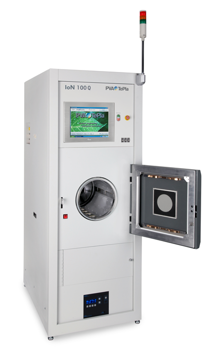
Featured Product