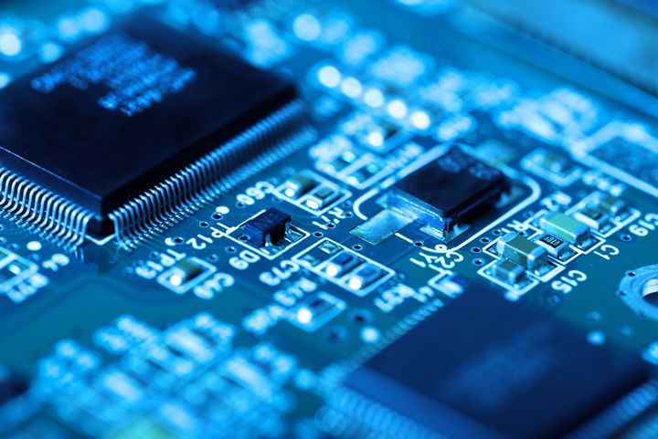
The miniature size of modern electronic components makes placement, mounting, soldering, and testing of said components rather difficult. Given their size and the overall component density on the PCB, visual inspection is nearly impossible.
 Inspecting Miniaturization: How 2D Laser Profilers Handle Tiny Electronic Components

Article from | KEYENCE
Semiconductors have become the backbone of modern electronics, allowing engineers to design and manufacture smaller, more power-efficient electronic devices with increasing computational capabilities. In fact, it’s safe to assume that this miniaturization in electronics has revolutionized our lives.
For example, the first commercially available mobile phone, the Motorola DynaTAC 8000X, weighed a hefty 2.5 pounds and stood 9 inches tall. It boasted a nickel-cadmium battery that provided approximately 30 minutes of talk time after a 10-hour charge.
The latest iPhone 15 Pro Max, on the other hand, weighs only 7.8 oz and measures only 6.30 × 3.02 × 0.33 inches. Not only is this smartphone smaller and significantly lighter than DynaTAC 8000X, but its technology, energy efficiency, and computational power are light years ahead.
It’s important to note that the DynaTAC 8000X’s board relied on surface-mount devices (SMDs) as components populating its main PCB, though at a density that could be inspected visually and with multimeter probes. However, the ongoing miniaturization of electronics took the iPhone further, and modern devices now must rely on modern inspection technologies.
The Challenges of Miniaturization
While the miniaturization of electronics made modern, powerful personal consumer electronics more compact, it also introduced a slew of challenges of its own. For example, a 6V 100µF through-hole capacitor has a dimensional volume of 1.5cm2, while that same capacitor in an SMD 0603 package has a dimensional volume of 0.34 mm2.
The miniature size of modern electronic components makes placement, mounting, soldering, and testing of said components rather difficult. Given their size and the overall component density on the PCB, visual inspection is nearly impossible. 2D profilers can help in this regard by scanning the PCB surface, allowing for easier detection of defects or abnormalities.
Defects and their Consequences
Defects in electronics design often have significant consequences on performance, reliability, and safety. A missing or misaligned component could cause a short circuit or inadequate currents to pass through other components, causing irreparable damage.
The most common defects associated with electronics and PCB manufacturing are component misalignment, soldering issues, cold joints (microcracks), and contamination. There are other issues as well, such as delamination, joint voiding, and electromigration, but those aren’t as closely related to component miniaturization as those previously mentioned.
Addressing the Challenges
The placement of electronic microcomponents is usually done by pick-and-place robots, which rely on machine vision for component positioning and orientation, significantly increasing the reliability of the production process.
The soldering process is usually done in so-called furnaces, and the whole process is machine-controlled. However, the miniaturization of electronic components presents real challenges when it comes to quality control, mainly due to the small size of the components and solder joints keeping them mounted to the PCB.
This is where 2D laser profilers, such as KEYENCE’s LJ-X8000 2D/3D Laser Profiler, come in. 2D profilers, also known as 2D scanners, are laser displacement sensors that, instead of measuring triangulation reflection, measure the displacement of the entire 2D scan line.
They achieve this by projecting a laser beam onto the surface of an object, which, in this case, is a PCB awaiting quality control. The light is reflected from the surface back into the photo-sensitive element housed inside the laser displacement sensor, and the measured data is compiled, processed, and stored for future analysis.
Thanks to their high precision and accuracy, which is often measured in the single-digit µm range, 2D scanners can detect component misalignment, component absence, or cracks in solder joints during quality control processes. This can trigger adequate rectification action or subsequent pre-rectification analysis by QC personnel.
The high precision of 2D profilers allows them to detect fine details and object contours, making them invaluable in dimensional measurements and critical for quality control and inspection applications.
The implementation of 2D profilers enhances quality control, which subsequently leads to higher-quality products and an overall reduction in manufacturing costs tied to rework and rectification.
Summary
The accuracy and precision of 2D profilers such as LJ-X8000 have found their use in electronics manufacturing and quality controls. As components continue to shrink in size, measuring their dimensions and position on a densely populated PCB has become nearly impossible to perform using manual inspection methods alone. Therefore, 2D laser profilers are indispensable for technological measurements in the future.
The content & opinions in this article are the author’s and do not necessarily represent the views of ManufacturingTomorrow
Featured Product

