Scanning Acoustic Microscopy Analyzes 3D Packages in the Z-dimension
The concept behind advanced 3D packaging is to stack multiple dies or wafers in a vertical direction – or Z-dimension – to achieve better performance with lower power requirements, smaller size and lower cost.
However, as 3D packages become increasingly complex, so do the challenges in identifying defects in multiple layers of stacked dies, silicon interposers and interconnections such as through-silicon vias (TSVs) and fine-pitch micro-bumps.
With less accessibility to internal components and a need to scan multiple, stacked layers, the focus is now shifting to methods of non-destructive testing both in manufacturing and for failure analysis.
3D Advanced Packaging
In general, the term 3D packaging applies to products manufactured by stacking silicon wafers or dies and interconnecting them vertically. This covers many integration schemes, including 3D wafer-level packaging, system in package (SiP), package on package (PoP), 2.5D and 3D, stacked ICs and other forms of heterogeneous integration.
To achieve vertical stacking, early 3D packages relied on interconnects such as wire bonding and flip chips. Today, communication between chips often involves a silicon or organic interposer or bridge, with TSVs. The interposer acts as the bridge between the chips and the board, while increasing the I/Os and bandwidth.
Now, the concept of chiplets is gaining momentum for advanced packaging. In this approach, modular chips – or chiplets – from third party vendors are used to build a package or system by stacking the components vertically.
By selecting the optimum CPU, IO, FPGA, RF or GPU, for example, the chiplets could be mix-and-matched using a die-to-die interconnect scheme involving a silicon interposer, a silicon bridge or high-density fan-out.
This approach has been embraced by Intel, which recently announced its new Foveros 3D packaging technology that allows complex, heterogenous logic chips to be stacked directly on top of each other.
Intel uses an active interposer instead of a typical passive silicon interposer. As an alternative, Intel is also offering its silicon bridge technology called Embedded Multi-die Interconnect Bridge (EMIB).
The Defense Advanced Research Projects Agency (DARPA), an agency of the U.S. Department of Defense, already plans to develop a large catalog of third-party chiplets for commercial, military and aerospace applications.
The goal of DARPA’s CHIPS program (Common Heterogeneous Integration and Intellectual Property Reuse Strategies) is to increase overall system flexibility and reduce design time by as much as 70%.
“The vision of CHIPS is an ecosystem of discrete modular, reusable IP blocks, which can be assembled into a system using existing and emerging integration technologies,” writes Andreas Olofsson in program information posted on the DARPA web site.
Still, there are challenges to making the chiplet concept work, including how to verify and test the individual chiplets from a variety of third-party vendors. Integrating multiple chiplets into stacked, 3D packages also requires high-density interconnections, all of which are potential sources of failure.
In comparison to other 3D package types, for example, stacked dies with through-silicon vias (TSV) require much smaller, finer pitch solder bumps that create additional challenges in defect detection.
Since any defective chiplets in the package will result in a non-functional package – even if all other modules are functional.
Given the combined value of the chiplets, interposer and other components, a single defective chiplet or poor interconnection can render the entire 3D package non-functional. This is driving the requirement for 100% inspection during manufacturing, ideally with non-destructive testing methods.
Non-Destructive Testing of 3D Packages
The challenge today is to perform 100% inspection with relatively high throughput to identify and remove 3D packages or components that do not meet quality requirements.
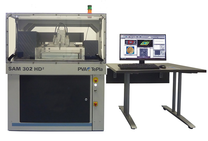
Among the available non-destructive methods, scanning acoustic microscopy (SAM) is the most widely used techniques for testing and failure analysis involving stacked dies or wafers.
SAM utilizes ultrasound waves to non-destructively examine internal structures, interfaces and surfaces of opaque substrates. The resulting acoustic signatures can be constructed into 3-dimensional images that are analyzed to detect and characterize device flaws such as cracks, delamination, inclusions and voids in bonding interfaces, as well as to evaluate soldering and other interface connections.
The unique characteristic of acoustic microscopy is its ability to image the interaction of acoustic waves with the elastic properties of a specimen. In this way the microscope is used to image the interior of an opaque material.
Scanning acoustic microscopy works by directing focused sound from a transducer at a small point on a target object. The sound, hitting a defect, inhomogeneity or a boundary inside material, is partly scatted and will be detected. The transducer transforms the reflected sound pulses into electromagnetic pulses which are displayed as pixels with defined gray values thereby creating an image.
To produce an image, samples are scanned point by point and line by line. Scanning modes range from single layer views to tray scans and cross-sections. Multi-layer scans can include up to 50 independent layers. Images from different depths can be combined into a single scan as well, called Tomographic Acoustic Micro Imaging (TAMI).
When even higher throughput is required, up to 4 transducers can simultaneously scan for higher throughput. Multiple transducers can be used on a single substrate and the images then stitched together, or multiple transducers can simultaneously scan multiple substrates.
“Scanning Acoustic Microscopy provides non-destructive imaging of defects and delaminations in die and package materials,” says Lisa Logan, Applications Manager Scanning Acoustic Microscopes for PVA TePla Analytical Systems, a company that designs and manufactures advanced Scanning Acoustic Microscopes for both laboratory and production environments.
“SAM is particularly useful for inspection of small, complex three-dimensional devices,” adds Logan. “The equipment is highly sensitive to the presence of delaminations and air-gaps at sub-micron thicknesses.”
The most common defects in 3D packaging are delamination, cracks in substrate, die tilt, misalignment and void in micro-bumps, bump defects, solder bridging, popcorn cracks, voids in underfill and voids and delamination in through-silicon vias (TSVs).
The resolution of microscopic image depends on the acoustic frequency, the material properties and aperture of the transducer. The frequency of the ultrasonic signals generated for 3D package inspection is typically within 15 to 300 MHz.
Transducers, the heart of all SAM systems, play such a critical role that manufacturers like PVA TePla Analytical Systems design and manufacture the transducers used in the equipment in a proprietary thin film technology process.
The frequency of the ultrasonic signals can even be increased into GHz range, which makes it possible to detect defects even in the sub-micron-range. PVA TePla’s high-resolution, GHz frequency SAM tool, for example, successfully detects voids in TSVs of 5-micron diameter and 50-micron depth, immediately after plating.
According to Logan, several leading suppliers of programmable logic devices have already evaluated and purchased high resolution SAM equipment for non-destructive analysis of next generation 3D products to scan for packaging anomalies.
“3D chip manufacturers are trying to push the limits on what they can detect, in terms of defects,” says Logan. “So, today the evaluation of scanning acoustic microscopy equipment often comes down to which equipment delivers the highest resolution at fastest throughput speeds for 100% inspection.”
Comments (0)
This post does not have any comments. Be the first to leave a comment below.
Featured Product